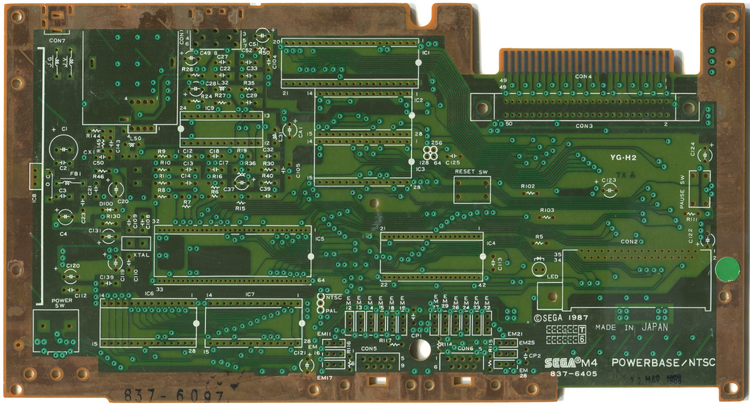
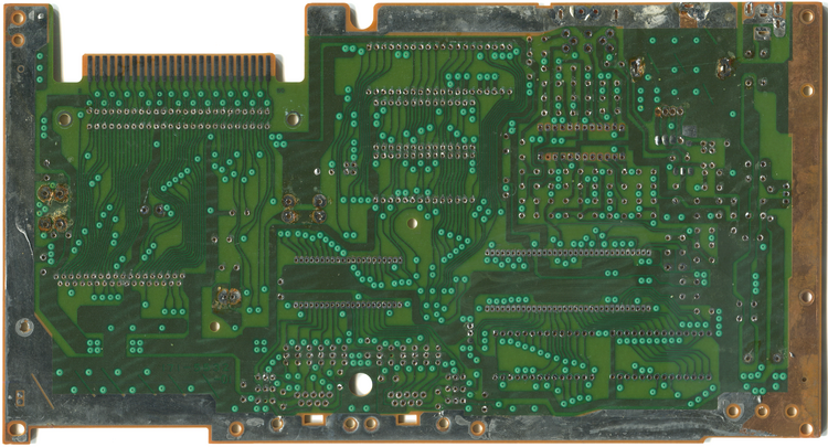
Designed in 1987 and introduced in early 1988, the 171-5532 (assembled part number 837-6405) is the second board revision for the NTSC model 1 Master System. It is functionally identical to the revision it replaces, but features a number of cost-reduction changes. All boards have the text SEGA M4 POWERBASE/NTSC 837-6405 silkscreened on the top, though the location seems to vary depending on which company fabricated the board. Boards fabbed by HDK have it located underneath the VRAM chips, while boards fabbed by TX have it underneath the card slot. The 171-5532 was produced between January and April of 1988.
One of the most noticeable changes is the use of the Sony CXA1145 video encoder, which replaced the Sony V7040 found in the previous revision. This slightly simplified the video circuitry as the single composite video output from the CXA1145 was run to both the RF modulator and DIN connector; the V7040 had two composite outputs which were both utilized in the previous revision. The PSG output was also run through the CXA1145's audio buffer, eliminating the discrete buffer transistor used before.
Both the Pause and Reset button switches were replaced with ALPS rubber tactile switches, which took up less internal space than the metal leaf switches used before. One slight improvement was made in the power circuitry as an unmarked diode was added on the input voltage rail and mounted across from the 7805 regulator, providing protection against an incorrect polarity AC adapter. The previous revision did not have any input protection, meaning that an incorrect power supply could damage the 7805 and prevent the system from powering on.
Perhaps the most drastic cost reduction came with the board itself, which is now made of phenolic resin (instead of FR-4) and has through-holes which are only plated at the bottom. The latter change contributes to this revision's lower reliability compared to the previous revision, particularly in regards to reading cartridges and cards as the solder joints for these connectors can easily crack if too much stress is placed on them. In addition, the solder pads on this revision (and all later NTSC boards) are incredibly fragile and will easily delaminate if too much heat or mechanical stress is applied to them. This can cause significant issues for modifications, repairs and capacitor replacement. Sega also left the top ground plane as bare copper instead of using a HASL (hot air solder leveling) finish.
This is seemingly the only NTSC board which was not repurposed for use in French consoles, as was the case with its predecessor and two succeeding board revisions. The 171-5532 would be replaced by both the 171-5538 and 171-5696 by mid-1988, making it one of the shortest-lived Master System board revisions in any region along with its PAL equivalent, the 171-5534.
Parts List
All resistors are 1/8 W.
| Designation | Value/Name | Notes |
|---|---|---|
| C1 | 100 uF 16V | |
| C2 | 0.1 uF | |
| C3 | 0.1 uF | |
| C4 | 100 uF 16V | |
| C12 | 0.1 uF | |
| C13 | 0.1 uF | |
| C14 | 0.1 uF | |
| C17 | 100 pF | |
| C18 | 0.01 uF | |
| C20 | 100 uF 10V | |
| C21 | 0.1 uF | |
| C22 | 47 pF | |
| C23 | 0.1 uF | |
| C25 | 100 uF 16V | |
| C27 | 100 nF | |
| C28 | 100 uF 16V | |
| C29 | 100 nF | |
| C32 | 100 nF | |
| C33 | 0.01 uF | |
| C37 | 10 uF 25V | |
| C39 | 0.1 uF | |
| C41 | 0.01 uF | |
| C49 | 10 uF 25V | |
| C51 | 100 uF 16V | |
| C52 | 100 nF | |
| C104 | 0.1 uF | |
| C105 | 0.1 uF | |
| C108 | 33 pF | |
| C109 | 33 pF | |
| C110 | 0.1 uF | |
| C112 | 0.1 uF | |
| C113 | 0.1 uF | |
| C119 | 10 uF 25V | |
| C120 | 10 uF 25V | |
| C121 | 10 uF 25V | |
| C122 | 47 uF 16V | |
| C123 | 47 uF 16V | |
| C124 | 47 uF 16V | |
| C125 | NP | |
| C131 | 10 uF 25V | |
| C139 | 150 pF | |
| C143 | 0.1 uF | |
| CA1 | 10 uF 25V | |
| CON1 | 8-pin DIN, 262 degree | Outputs composite video, mono audio and RGB |
| CON2 | Sega 209-5020 | Card slot, same part as used in the Mark III |
| CON3 | 50-pin edge connector, 2.54 mm pin pitch | Cartridge slot |
| CON5 | 9-pin D-sub connector | 1P port |
| CON6 | 9-pin D-sub connector | 2P port |
| CON7 | 5.5 x 2.1 DC barrel jack | Power input |
| CP1 | 0.1 uF | |
| CP2 | 0.1 uF | |
| CX1 | 180 pF | |
| D100 | 1S2473 | |
| EM11 | 2200 pF line filter | |
| EM12 | 2200 pF line filter | |
| EM13 | 2200 pF line filter | |
| EM14 | 2200 pF line filter | |
| EM15 | 2200 pF line filter | |
| EM16 | 2200 pF line filter | |
| EM17 | 270 pF line filter | |
| EM18 | 2200 pF line filter | |
| EM19 | 2200 pF line filter | |
| EM21 | 2200 pF line filter | |
| EM22 | 2200 pF line filter | |
| EM23 | 2200 pF line filter | |
| EM24 | 2200 pF line filter | |
| EM25 | 2200 pF line filter | |
| EM26 | 2200 pF line filter | |
| EM27 | 270 pF line filter | |
| EM28 | 2200 pF line filter | |
| EM29 | 2200 pF line filter | |
| FB1 | Ferrite bead, no value | |
| IC1 | Zilog Z0840004PSC | CPU |
| IC2 | Sharp MPR-10052 or Sony CXK3864 | v1.3 BIOS |
| IC3 | NEC D4168C-20 | Z80 RAM |
| IC4 | Sega 315-5216 | I/O controller |
| IC5 | Sega 315-5124 / Yamaha YM2602 | VDP |
| IC6 | NEC D4168C-15 | VRAM |
| IC7 | NEC D4168C-15 | VRAM |
| IC8 | 7805 | Voltage regulator |
| IC9 | Sony CXA1145 | Video encoder |
| JG | Ferrite bead, no value | |
| JV | 10 uH | |
| L31 | 39 uH | |
| L32 | 39 uH | |
| L50 | 100 uH | |
| LED | Green LED | |
| PAUSE SW | ALPS SKEEVA[1] | |
| POWER SW | Sega 509-5150 | Made by Mitsumi, nearly identical to and compatible with the NES front loader power switch |
| R5 | 120 ohm | |
| R6 | 2.2k ohm | |
| R7 | 2.2k ohm | |
| R8 | 2.2k ohm | |
| R9 | 4.7k ohm | |
| R10 | 4.7k ohm | |
| R11 | 4.7k ohm | |
| R15 | 10k ohm | |
| R16 | 1k ohm | |
| R19 | 2.2k ohm | |
| R24 | 75 ohm | |
| R26 | 10k ohm | |
| R27 | 2.2k ohm | This factory value is incorrect and provides a dark and oversaturated picture over composite; a 1k or 1.2k ohm resistor will provide improved video quality |
| R30 | 1.2k ohm | |
| R35 | 1k ohm | |
| R36 | 24k ohm | |
| R40 | 1k ohm | |
| R46 | 2.2k ohm | |
| R47 | 10k ohm | |
| R50 | 75 ohm | |
| R102 | 4.7k ohm | |
| R103 | 4.7k ohm | |
| R108 | 4.7k ohm | |
| R111 | 4.7k ohm | |
| R114 | 330 ohm | |
| R115 | 330 ohm | |
| R116 | 330 ohm | |
| R117 | 330 ohm | |
| R130 | 100k ohm | |
| R144 | 10k ohm | |
| R145 | 2.2k ohm | |
| RESET SW | ALPS SKEVVA[2] | |
| RF | Jalco MGB3-VU3401 (some boards) | |
| XTAL | 10.7386 MHz | |
| Unmarked | Diode | For reverse polarity protection |