 | This is an advanced mod. If care is not taken while removing the original memory chip, multiple solder pads can be lifted, which will result in an extremely difficult repair being necessary. The key to avoiding this is patience. |
The Sega CD holds saved games in a static RAM (SRAM) chip on its motherboard. The SRAM chip requires constant power in order to retain the game saves, which an on-board coin cell battery supplies. Some systems such as the JVC X'Eye use a supercapacitor in place of a battery. In the event that the battery dies or the supercapacitor loses charge, all game saves will be lost.
However, it was discovered that the SRAM chip can be replaced with a ferroelectric RAM (FRAM) chip which retains information regardless if power is available or not — and optionally, a larger capacity FRAM chip can be used in combination with physical switches to four separate data banks. A replacement BIOS is also available which allows the entire capacity of the FRAM chip to be seen by the BIOS, allowing for quadruple the capacity of memory blocks.
This mod applies to all Sega CD variants, including the LaserActive Sega PAC, all combination consoles (i.e. X'Eye, both Wondermegas, CDX), and even the Aiwa Mega CD.
Choosing Chip
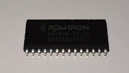
First, choose a FRAM chip to replace the stock one with. Replacement chip candidates include:
- FM16W08-SG - 64 KB (matches stock SRAM size, go with this unless you plan on bankswitching or a replacement BIOS)
- FM18W08-SG - 256 KB (extra space is not seen by the stock BIOS, but can be bankswitched or used with a replacement BIOS which can access the extra space)
- Some chips are sold without "-SG" on the end. -SG signifies that the chip is a SOIC package type (instead of -PG which is through-hole, not suitable for this mod).
Required Materials
- Tools
- Soldering iron
- Hot air rework station (optional, can be substituted for low melt solder)
- Multimeter with continuity mode
- Tweezers
- Philips head screwdriver
- Materials
- FRAM chip (either FM16W08 or FM18W08)
- Two SPDT switches (or one DPDT switch)
- Insulated wire or magnet wire
- Leaded solder
- Low melt solder (if not using hot air station)
- Flux
- Desoldering braid
- Isopropyl alcohol (at least 90%)
- Cleaning swabs (microfiber/foam are better than cotton since they don't leave strands behind)
Procedure
Removing SRAM Chip
- Disassemble the console and pull out the motherboard.
- Locate the SRAM chip. It should be marked either:
- MB8464A-10L (Model 1 or Funai-produced Model 2 - IC 112)
- MB8464A-80L or XL J6265AF-10SL (Sega-produced Model 2 - IC 112)
- MB8464H-10LL (Aiwa Mega CD)
- LC3664BML-10 (Sega CDX; note that there are two LC3664BML-10 chips. Replace IC10.)
- MS6264CLL-10FC (PAC-S1/S10)
- LC3564QM (Wondermega, Wondermega M2 and JVC X'Eye)
- Cover nearby components with kapton tape or foil to protect them from heat.
- Instead of using a hot air station, you can also use low temperature solder such as Chip Quik to remove the SRAM chip. This is especially recommended for the Aiwa Mega CD which has a motherboard that is very sensitive to heat. Use desoldering braid to thoroughly clean up the Chip Quik as it can contaminate your solder joints when the FRAM chip is soldered in.
- On the X'Eye, the SRAM chip is epoxied to the bottom of the motherboard and must be removed using hot air. Alternatively, a flex adapter can be soldered in without needing to remove the SRAM chip.
- Turn on the hot air rework station and set it to 360 degrees Celsius with medium air flow.
- Start by preheating the chip from a distance of 4-5 inches with the hot air station and very evenly distribute the heat around the chip for 30 seconds or so.
- Next, circle the perimeter of the chip with your hot air nozzle, making sure not to apply heat to any one location for too long.
- Have patience. This will take time, especially if the chip has adhesive underneath it (which is present on the X'Eye). The hot air at this temperature should not hurt the board as long as it is evenly applied.
- While continuing the previous step, check if the chip has loosened with tweezers or another small implement by grabbing the side of the chip and gently try to lift without applying force. Once the chip is ready, it will easily come off.
- Warning: If force is applied here, pads and traces may pull up along with the chip!
- Once the chip eventually separates from the board, turn off the hot air rework station.
- Turn on the soldering iron and wick up any remaining solder on the pads with solder wick to make an even surface. Use flux to help make this process easier.
Installing FRAM Chip
- If using an FM18W08 and are planning on bankswitching or an alternative BIOS, lift both pins 1 and 26 as these are the address pins that will be attached to switches.
- Place the chip on the board. The orientation of the chip should match the marking on the board.
- Line up the legs with pads on the board, and apply some flux to one corner.
- Once satisfied, tack one leg down with the soldering iron to fix the chip in place.
- It may help to gently rest a finger or tape on top of the chip to hold it in place while you tack the first leg down.
- Repeat on the diagonally opposite corner of the chip to anchor the chip.
- Apply a generous amount of flux, and then solder the rest of the legs down with a dragging technique.
- Ensure that all legs (aside from pin 1 and pin 26 if bankswitching) are soldered to the pads on the board with good solder joints.
- Use the multimeter to double check that no legs are bridged with their neighbor pins, and that all legs have good connections to the board.
- If using an FM18W08, make sure to wire pins 1 and 28 together if you are not bankswitching.
- Clean up any excess flux with some isopropyl alcohol and swabs.
- Optionally, the original save battery or supercapacitor can be removed as it will now be redundant.
- Put the Sega CD console back together enough to connect to the Sega Genesis and test.
- Power on the console and format the system memory from the BIOS (dependent on Sega CD model and region). This will need to be done in order to make the system memory usable, and some games will actually crash if you do not perform this step (i.e. Popful Mail).
- On the model 2 Sega CD and CDX/Multi-Mega, you will need to insert a game disc first and then press button A to access the system menu.
- Play a game and save some data to the memory.
- Power off the console and disconnect the power for at least 30 seconds.
- Power it back on and verify that the memory is still saved. If so, the installation is complete.
-
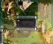 The original SRAM chip on a JVC X'Eye is being prepared for removal. Kapton tape has been laid around the chip to protect other components from being damaged or accidentally removed by hot air.
 -
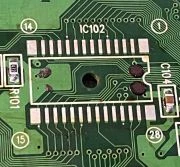 With the SRAM chip removed, the pads can be wicked clean.
 -
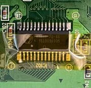 An FM18W08 is being prepared for soldering. A strip of Kapton tape has been placed on the chip to help keep it aligned onto the pads.
 -
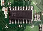 A completed FRAM install on an X'Eye. Pin 28 (5V) has been tied to pin 1 (A14) with a small piece of magnet wire since it is an unused address line.
Enabling Bankswitching
 | For the FM18W08 only! |
- Identify nearby solder points to get ground and 5V. Depending on the location of the chip, a good ground point might be one of the various exposed points on the edge of the board. Use a multimeter in continuity mode to identify a 5V point. The power supply connector in the corner of the motherboard is a great place to start with testing for this.
- Touch one probe of the multimeter to the 5V pin on the connector, and then use the other probe to test other nearby solder points until the multimeter produces a long tone. This could be a leg on a chip, capacitor, test pad, etc.
- Solder a wire from pin 1 to switch 1, and two more wires from the switch to GND and 5V to allow pin 1 to be switched between GND and 5V.
- Solder a wire from the already-lifted pin 26 to switch 2, and two more wires from the switch to GND and 5V to allow pin 26 to be switched between GND and 5V.
- Test each bank by powering it on, saving data to it, powering it off, changing flipping switches to a different position, and repeating for each bank; verifying that no data is lost when you revisit a bank.
Extended Memory BIOS
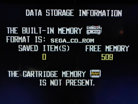
In 2023, Leo Oliveira (building on initial research from Russell Quigley), developed an alternative BIOS which, in addition to making a Sega CD system almost region-free, can access the entire 256 kilobit (32 kilobyte) capacity of an FM18W08 chip at once, expanding the system storage from 125 to 509 blocks. This is especially useful for RPGs which use a large number of blocks; Shining Force CD in particular benefits from this modification as it means the entire game can be completed without needing a RAM cartridge. For the region-free aspect, the only games which are still not completely compatible are Flashback (this also detects the host console's region) and Sensible Soccer.
To enable this functionality, pins 1 and 26 of the FM18W08 (address bits 14 and 13 respectively) must be connected to the 68000 CPU. Without this extra modification, the system can only address the standard 64 kilobits (8 kilobytes) of memory. This modification can be performed on all consoles, details on performing a BIOS replacement can be found in the CD BIOS Mod procedure. Note that this modification does not necessarily require an FRAM chip, as the original battery or supercapacitor can be used with a larger capacity SRAM chip.
An archive of all versions of this BIOS can be downloaded here. Make sure to only use the BIOS that matches the particular model you have (i.e. you cannot use a BIOS meant for a model 1 on a model 2 and vice versa).
Procedure
- Follow the CD BIOS Mod procedure in its entirety. All of the BIOSes included in the archive must be byteswapped before burning to an EPROM, or the system will not work at all. Note that this process will vary depending on the particular model.
- Information on performing this mod on a LaserActive PAC-S1/S10 can be found in this procedure.
- Make sure to use the BIOS that matches the particular model you have. This is especially important for the model 2 as the earliest version of its BIOS only works on Funai-produced systems (MK-4102, MK-4102-50 or HAA-2912).
- If not already done, lift pin 26 of the save RAM chip clear of the board. Pin 1 is normally not connected and does not need to be lifted.
- Alternatively, pin 10 of the MB3790 power management chip can be lifted in lieu of pin 26 of the save RAM. If using an FRAM chip, the MB3790 can be removed entirely since it was only responsible for regulating battery power to the original SRAM chip.
- Use thin gauge wire to connect pin 1 of the save RAM chip to pin 46 of the 68000 (A14), then connect pin 26 of the save RAM chip to pin 45 of the 68000 (A13).
- Put the Sega CD console back together enough to test.
- Power on the console and format the system memory from the BIOS (dependent on Sega CD model and region). This will need to be done in order to make the system memory usable, and some games will actually crash if you do not perform this step (i.e. Popful Mail).
- When formatted, the system should state that 509 blocks of memory are free. If the system still only shows 125 blocks or cannot format the save RAM, double check the installation and test again.
- On the model 2 Sega CD and CDX/Multi-Mega, you will need to insert a game disc first and then press button A to access the system menu.
- Play a game and save some data to the memory.
- Power off the console and disconnect the power for at least 30 seconds.
- Power it back on and verify that the memory is still saved. If so, the installation is complete.
-
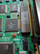 An expanded save RAM mod in a model 1 Mega CD, using a FM1808 FRAM chip.
 -
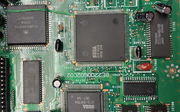 The same mod in a model 2 Sega CD.
 -
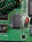 Closeup of a model 2 install, with emphasis on the FRAM wiring.
 -
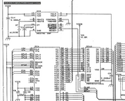 A section of the model 1 schematic, giving an overview of the save RAM and battery connections.
 -
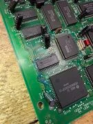 FRAM install in newer Sega CD 2 unit showing how pin 1 and 26 on the FRAM connect to the 68000 CPU
Troubleshooting
Sometimes installations go wrong. It happens. Here's a few tips to try and salvage things if it doesn't work the first time.
- Double check that no adjacent pins are shorted together.
- Double check that all pins are connected to the solder pads.
- Follow the trace of each leg of the chip and verify continuity if possible.
- Some traces might go to a via that's underneath another chip. It should be accessible on the other side of the board.
- If there isn't continuity, the solder pad might have been lifted, and a jumper wire may be necessary.
- Verify that the lifted legs / conducting wires aren't shorting on the RF shielding of the case.